- 您现在的位置:买卖IC网 > Sheet目录480 > MTB75N05HDT4 (ON Semiconductor)MOSFET N-CH 50V 75A D2PAK-3
�� �
�
�MTB75N05HD�
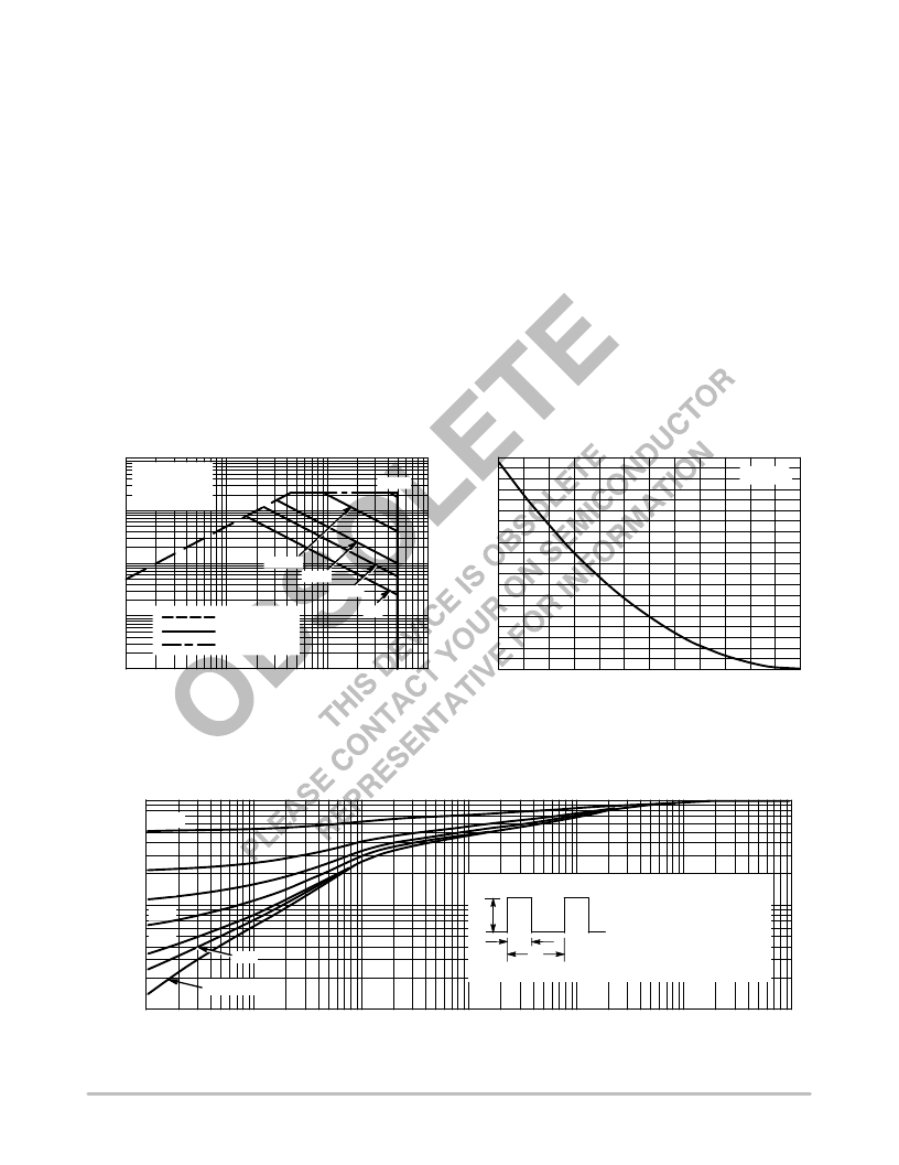
�SAFE� OPERATING� AREA�
�The� Forward� Biased� Safe� Operating� Area� curves� define�
�the� maximum� simultaneous� drain� ?� to� ?� source� voltage� and�
�drain� current� that� a� transistor� can� handle� safely� when� it� is�
�forward� biased.� Curves� are� based� upon� maximum� peak�
�junction� temperature� and� a� case� temperature� (T� C� )� of� 25� °� C.�
�Peak� repetitive� pulsed� power� limits� are� determined� by� using�
�the� thermal� response� data� in� conjunction� with� the� procedures�
�discussed� in� AN569,� “Transient� Thermal� Resistance� ?�
�General� Data� and� Its� Use.”�
�Switching� between� the� off� ?� state� and� the� on� ?� state� may�
�traverse� any� load� line� provided� neither� rated� peak� current�
�(I� DM� )� nor� rated� voltage� (V� DSS� )� is� exceeded,� and� that� the�
�transition� time� (t� r� ,� t� f� )� does� not� exceed� 10� μ� s.� In� addition� the�
�total� power� averaged� over� a� complete� switching� cycle� must�
�not� exceed� (T� J(MAX)� ?� T� C� )/(R� θ� JC� ).�
�A� power� MOSFET� designated� E� ?� FET� can� be� safely� used�
�in� switching� circuits� with� unclamped� inductive� loads.� For�
�reliable� operation,� the� stored� energy� from� circuit� inductance�
�dissipated� in� the� transistor� while� in� avalanche� must� be� less�
�than� the� rated� limit� and� must� be� adjusted� for� operating�
�conditions� differing� from� those� specified.� Although� industry�
�practice� is� to� rate� in� terms� of� energy,� avalanche� energy�
�capability� is� not� a� constant.� The� energy� rating� decreases�
�non� ?� linearly� with� an� increase� of� peak� current� in� avalanche�
�and� peak� junction� temperature.�
�Although� many� E� ?� FETs� can� withstand� the� stress� of�
�drain� ?� to� ?� source� avalanche� at� currents� up� to� rated� pulsed�
�current� (I� DM� ),� the� energy� rating� is� specified� at� rated�
�continuous� current� (I� D� ),� in� accordance� with� industry�
�custom.� The� energy� rating� must� be� derated� for� temperature�
�as� shown� in� the� accompanying� graph� (Figure� 12).� Maximum�
�energy� at� currents� below� rated� continuous� I� D� can� safely� be�
�assumed� to� equal� the� values� indicated.�
�1000�
�100�
�V� GS� =� 20� V�
�SINGLE� PULSE�
�T� C� =� 25� °� C�
�10� μ� s�
�500�
�450�
�400�
�350�
�I� D� =� 75� A�
�300�
�10�
�1�
�100� μ� s�
�R� DS(on)� LIMIT�
�THERMAL� LIMIT�
�1� ms�
�10� ms�
�dc�
�250�
�200�
�150�
�100�
�PACKAGE� LIMIT�
�50�
�0.1�
�0.1�
�1�
�10�
�100�
�0�
�25�
�50� 75� 100� 125�
�150�
�175�
�1�
�V� DS� ,� DRAIN?TO?SOURCE� VOLTAGE� (VOLTS)�
�Figure� 12.� Maximum� Rated� Forward� Biased�
�Safe� Operating� Area�
�D� =� 0.5�
�0.2�
�T� J� ,� STARTING� JUNCTION� TEMPERATURE� (� °� C)�
�Figure� 13.� Maximum� Avalanche� Energy� versus�
�Starting� Junction� Temperature�
�0.1�
�0.1�
�0.05�
�P� (pk)�
�R� θ� JC� (t)� =� r(t)� R� θ� JC�
�R� θ� JC� =� 1.0� °� C/W� MAX�
�D� CURVES� APPLY� FOR� POWER�
�0.02�
�0.01�
�t� 1�
�t� 2�
�DUTY� CYCLE,� D� =� t� 1� /t� 2�
�PULSE� TRAIN� SHOWN�
�READ� TIME� AT� t� 1�
�T� J(pk)� ?� T� C� =� P� (pk)� R� θ� JC� (t)�
�SINGLE� PULSE�
�0.01�
�1.0E?� 05�
�1.0E?� 04�
�1.0E?� 03�
�1.0E?� 02�
�1.0E?� 01�
�1.0E+00�
�1.0E+01�
�t,� TIME� (s)�
�Figure� 14.� Thermal� Response�
�http://onsemi.com�
�6�
�发布紧急采购,3分钟左右您将得到回复。
相关PDF资料
MTCBA-C1-N3
MODEM CDMA RS232 DUAL
MTCBA-C1-U-N2
MODEM CDMA USB 800MHZ 1.9GHZ
MTCBA-C1X-N2-NAM
MODEM CDMA 800MHZ 1.9GHZ
MTCBA-G-EN-F4-ED-GB/IE
MODEM GPRS QUAD EU/UK ETH INTFC
MTCBA-G2
MODEM GPRS CELLULAR SERIAL
MTCBA-H-EN2-NAM
WIRELESS ROUTER INTELLIGNT HSDPA
MTCBA-H3-U1
MULTIMODEM CELL WIRELESS MODEM
MTCBA-H4-EN2-GP-P1
ROUTER WIRELESS QUAD HSPA
相关代理商/技术参数
MTB75N06
制造商:MOTOROLA 制造商全称:Motorola, Inc 功能描述:TMOS POWER FET 75 AMPERES 60 VOLTS
MTB75N06HD
制造商:ON Semiconductor 功能描述:Trans MOSFET N-CH 60V 75A 3-Pin(2+Tab) D2PAK Rail
MTB7671
制造商:Megger 功能描述:METER TEST BOX
MTB-7PL80
制造商:ITT Interconnect Solutions 功能描述:MTB-7PL80 / 095262-0006 / MICRO
MTB-7SL80
制造商:ITT Interconnect Solutions 功能描述:MTB-7SL80 - Bulk
MTB8N50E
制造商: 功能描述: 制造商:undefined 功能描述:
MTB90P06J3
制造商:CYSTEKEC 制造商全称:Cystech Electonics Corp. 功能描述:P-Channel Logic Level Enhancement Mode Power MOSFET
MTB95255-58
制造商:ITT Interconnect Solutions 功能描述:MTB95255-58 / 095255-0058 / Micro